BRIDGELESS POWER FACTOR CORRECTION CIRCUITS
Conventional power factor correction (PFC) circuits for SMPS contain an input rectifier bridge. As the result, at any given moment the AC line current flows through three semiconductor components- two diodes of the bridge and then either a switch (such as a FET) or boost diode.
The diagram below shows a conceptual schematic of the original BPFC described in U.S. Patent 4,412,277 (1983).
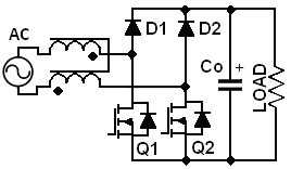 During positive half-cycle the power is processed by the cell formed with Q1 and D1. The current returns through Q2, which plays a role of a rectifier. During negative half-cycle the boost is formed with Q2, D2 and the return pass is Q1. We can see that compared to the conventional off-line boost converter, one diode is eliminated from the circuit, which results in reduced conduction losses. Both Q1 and Q2 can be driven with the same PWM signal, which simplifies the control. The disadvantages of this architecture are the inconveniences in monitoring inductor current waveform and sensing the input voltage, which are actually common drawbacks of most BPFC.

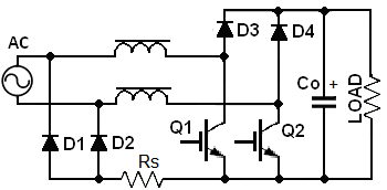
A modification of the above circuit with a bidirectional switch was proposed by Delta (US20070279955 A1). During "ON" time the current flows through Q1, Q2. During "OFF" time it flows though either D1 and D4 or D2 and D3. So, at any given moment there only two semiconductors in the current path. This arrangement however presents an additional issue of driving floating MOSFETs with a pulse sequence whose duty cycle can vary from 0 to 1.
 This variation of the bridgeless circuit has two boost channels, one for each half-line cycle. Unlike previous topologies, this one requires two separate inductors. However this approach has a big advantage- both Q1 and Q2 here are referenced to the same common and you can use a single current sense resistor with a conventional PFC controller. You may just need to use IGBTs instead of FETs to prevent return current of one channel from flowing through body diode of the other one.
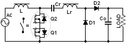
A resonant BPFC was proposed by Dr.Ćuk (US20100259240 A1).
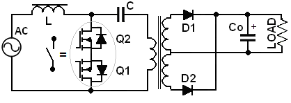
 Although the image in his patent application shows a single switch, it has to a bi-directional one, so in reality it will consist of two back to back MOSFETs switches (Q1 and Q2). This configuration is claimed to be a "true" bridgeless PFC, but we can see that during conduction state the current still flows through three devices: Q1, Q2 and D1. At low line where duty cycle is high and losses are highest, this configuration hardly has any advantage over other topologies.
This is an example of discontinuous mode isolated BPFC based on SEPIC converter.
Note that all BPFC require twice the amount of the semiconductor switches compared to conventional PFC boost. If you take a conventional circuit and double the amount of FETs by paralleling them, you can as well reduce the conduction losses without complicating the circuit. That's why if you consider using a BPFC, I feel you should compare its efficiency with that of a regular circuit with the same FETs count.
Legal: some of the circuits shown here may be patented- read the disclaimer linked below.