DESIGN OF CCM POWER FACTOR CORRECTION BOOST CONVERTER

The main advantage of continuous mode boost is lower ∆iL and lower peak current to average ratio. This reduces conduction losses and requires smaller EMI filter. The main disadvantage is hard reverse recovery of the free-wheeling diode. This process generates high-frequency noise in the range of tens of megahertz and increases switching losses. Continuous mode of operation is typically used in SMPS with power levels greater than 100W. To the left is a conceptual schematic and timing diagrams of CCM boost. Below we'll derive the main design equations and provide a quick calculator of the the rms currents and the required inductor value. Let's start with inductor volt-second balance during each switching cycle "T":
Vin×ton=(Vo-Vin)×toff (1)
Note that since the average current is continuously changing according to the input voltage, strictly speaking, volt-seconds across "L" are not exactly balanced. However, because normally, the switching frequency Fsw is at least three orders of magnitude higher than mains frequency, we can neglect net current change over one switching cycle.
If D - duty cycle, then ton=DT and toff=(1-D)T. Substituting this into (1) we find:
D=1-Vin/Vo (2)
From (2) we can derive current ripple:
∆iL=Vin×ton/L = Vin(Vo-Vin)/L×Fsw×Vo (3),
where Fsw=1/T- switching frequency.
In the equations (1)-(3) Vin is instantaneous value of input voltage. It is varying continuously with AC phase angle Φ(t) according to the following equation:
Vin(Φ)=√2×Vrms×|sinΦ|, where Φ(t)=2π×f×t, f- line frequency.
It is easy to determine from (3) that ∆iL reaches maximum when instantaneous value of the input sine wave is equal to Vout/2.
The condition of continuous conduction mode is ∆iL/2<ILpk, where ILpk - peak value of filtered line-frequency current (shown in blue in our diagram).
Assuming perfect power factor correction (PF=1.0):
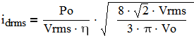
ILpk = √2×ILrms = √2×Po/(Vrms×η) (4),
where Po- output power, η - efficiency in decimal. Therefore for CCM at certain Vinrms the inductance should satisfy the following equation:
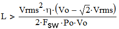
(5)
In practice, the designers often select "L" value such that at low line ∆iL<20...60% of Ipk, so practically "L" is selected several times larger than the result from (5). With such selection, at higher input voltages the current ripple ratio will be higher and the converter may even become discontinuous.
Let's now calculate the currents in this circuit. These numbers can be used for components selection and for thermal design. For simplicity we will assume that L is sufficiently large so we can neglect ∆iL. Since the switch (which is usually a FET) conducts only during the DT portion of the period T, its RMS current during one switching period is IQrms(Φ)=IL(Φ)×√D(Φ). All quantities here vary with the phase angle Φ of input voltage. Substituting (2) and (4) into the above expression yields:
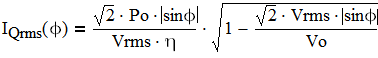
(6)
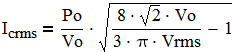
Then IQmrs averaged over entire period of input AC is:
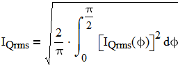
(7)
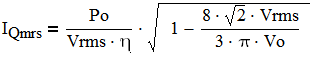
(8)
The above value determines conduction losses in the FET.
The boost diode conducts during (1-D)T time. Therefore during each switching cycle Idiode_rms(Φ)=IL(Φ)×√(1-D(Φ)). By considering the integral of Idiode_rms(Φ) squared similar to (7), the RMS diode current can be calculated as follows:
(9)
The rectifier should selected based on the Vo and idrms. It is important to note that when it turns off, its reverse recovery current causes significant switching losses and generate noise in the range 30 to 50 MHz. Therefore the diode should be selected with ultra fast soft switching characteristic. The best performance for this application is achieved by silicon carbide (SiC) diodes.
Output capacitor is charging when the diode conducts and is discharging to the load when "Q" is ON. Assuming the load consumes fixed DC current Po/Vo, we can find the total capacitor current:
(10)
The capacitor current contains two components: twice line frequency and switching frequency:
Ic_2F_rms=Po/(Vo√2) (11)
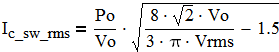
(12)
The capacitor should be selected to handle Ic_2F_rms and Ic_sw_rms. Its capacitance should be enough to provide during power interruptions the required hold up time at a given load Po.
This online calculator will provide you with basic power relationship for the boost converter design. For an example of complete power stage design see the schematic of 300W active CCM PFC pre-regulator.
For complete design information get my SMPS design handbook.